Electronics Anywhere
Tom Jackson, Robert E. Kirby Chair Professor of Electrical Engineering
Center for Thin Film Devices and Materials Research Institute
Department of Electrical Engineering
Pictured
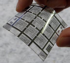
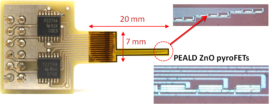
Top:ZnO thin film transistors (TFTs) and circuits fabricated on a polyester (PET) substrate with ZnO and Al2O3 thin films deposited by plasma enhanced atomic layer deposition. Bottom: Temperature sensor for implantable medical use. The sensor uses ZnO TFTs as sensing and control devices.
The history of the electronics industry over the past four decades or more has been largely an elaboration of Moore’s Law: the doubling of integrated circuit transistor density every two years or so. The scale of the success of the semiconductor industry to produce ever more complex circuits with ever decreasing cost per circuit element can be difficult to comprehend. More than 1020 transistors, in all forms, were sold last year, about 3 transistors for each mm of the distance between earth and the nearest star, or more than one hundred transistors for every grain of sand on all the earth’s beaches.
The historic Moore’s Law path has resulted in greater and greater facility in putting complex active electronics in only one place: single crystal semiconductor surfaces. Of course those surfaces can be put in diverse locations to solve a wide variety of problems. Today, digital computation, and increasingly signal processing and communication are, to first order, free on the scale of the problems they are employed to solve. But many problems are not amenable to a Moore’s Law type solution. For example, at the 22 nm technology node the number of active devices required for a HD1080 color active matrix display (1920 × 1080 pixels) can be fabricated in less than one square mm. But fractional mm displays have limited interest and sales prospects. From a device perspective this has resulted in an interesting situation. From the standpoint of economic importance Si MOSFETs (and variants) are number one by a wide margin. But hydrogenated amorphous silicon thin film transistors (a-Si:H TFTs), used for displays and which have followed a distinctly non-Moore’s-Law path, are number two.
Jackson’s research group aims at generalizing non-Moore’s Law active thin film electronics for applications far beyond displays. Imagine an electronic dressing applied after a surgical resection that can provide pixel-by-pixel diagnostics, drug therapy, or imaging, and then would be absorbed when no longer needed. Or infrastructure sensors that can be built into new bridges or buildings, or applied to old, that can harvest locally available energy (from light, temperature gradients, or vibrations), sense changes or failure conditions, and broadcast status or warning to nearby receivers. Or food freshness sensors that monitor for E. coli or other hazards and assist vendors in storing and rotating goods. The technology to enable all of these is emerging. Jackson’s research group focuses on the active devices, mainly transistors, and processes which can enable such new applications. Work includes thin film transistors (TFTs) using organic or oxide semiconductors. Organic semiconductors are not those produced without chemicals, but rather semiconductors composed of organic materials (more familiar as wire insulation or plastic packaging) instead of inorganic materials like silicon or gallium arsenide. Organic semiconductors allow device fabrication at low temperature and integration with low temperature materials like plastic substrates. They also have many characteristics, for example hardness, stiffness, and thermal conductivity, much closer to biological systems (tissue, cells) than conventional inorganic semiconductors. Oxide semiconductors use materials like zinc oxide, familiar as a component in white paste type diaper ointment, as the active semiconductor material. Oxide semiconductors also allow device fabrication at low temperature and on unconventional substrates and provide performance advantages compared to organic semiconductors.
The Jackson group labs contain equipment to build devices and circuits using unconventional semiconductors and substrates from concept to real-world demonstrations. This includes material deposition techniques like atomic layer deposition (ALD) that allows sub-nanometer control of deposited layer thickness, tools to handle and do micron scale patterning on flexible substrates, and tools to image and characterize devices with nanometer resolution. Jackson group students frequently blaze new trails for device design and processing and become well-practiced problem solvers. They have been hired by a diverse range of employers including Intel, IBM, HP, Agilent, Texas Instruments, Cadence, NIST, and the Max Plank Institute.